![[Free Support] Key Points for Selecting Probes for Circuit Board Inspection](https://image.mono.ipros.com/public/product/image/203351/IPROS12893495888806362962.png?w=280&h=280)
[Free Support] Key Points for Selecting Probes for Circuit Board Inspection
Choosing the wrong probe can lead to misjudgments and damage to the circuit board?! We will measure the contact resistance and select the most suitable probe for the measurement target and conditions.
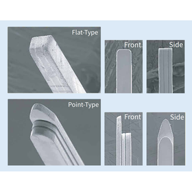
The selection of contact probes for substrate inspection needs to be done carefully. Although it is referred to as for substrate inspection, there are various contact points such as through holes, leads, and bus bars. The optimal probe can vary greatly depending on the shape and material of these contact points. If the selection is incorrect, there is a risk of reduced inspection yield due to misjudgment caused by poor contact, or even damage to the substrate. There are mainly two key points for selecting the appropriate probe: 1. Tip shape: If it is not suitable for the shape or material of the contact point, there is a possibility of electrical contact failure or physical inability to make contact. 2. Spring load: If it is too weak, stable contact cannot be achieved, leading to misjudgment. Conversely, if it is too strong, there is a risk of damaging the substrate. However, there are many customers who are troubled by the question, "Which one is optimal for our measurement points?" Therefore, Sankei Engineering offers a free probe selection service that utilizes our expertise as a probe manufacturer. We take your workpieces and measure the contact resistance values using our own equipment. Based on that data, we select and propose the optimal probe. Inquiries during the information-gathering stage are also welcome. Please feel free to consult us through the inquiry form.
- Company:サンケイエンジニアリング 本社
- Price:Other